PCF8591 is a single chip integrated,
single power supply, low power consumption, 8-bit CMOS data acquisition
device.PCF8591 has four analog inputs, one analog output, and one serial I2C bus
interface.The three address pins A0, A1, and A2 of PCF8591 can be used for
hardware address programming, allowing access to eight PCF8591 devices on the
same I2C bus without additional hardware.The input and output address, control
and data signals on the PCF8591 device are transmitted serially through a
two-wire bidirectional I2C bus.
Main performance indicators of
PCF8591:
Br single power supply
Process PCF8591 operating voltage
range 2.5v -6V
Shorter standby current
Matlab serial input/output through
the I2C bus
Matlab PCF8591 addresses through
three hardware address pins
The sampling rate of matlab PCF8591
is determined by the I2C bus rate
The four analog inputs are
programmable to be single - end or differential inputs
Creeping automatic incremental
channel selection
The simulated voltage range of matlab
PCF8591 is from VSS to VDD
Matlab PCF8591 has a built-in
tracking and holding circuit
Shorter 8-bit approximates A/D
converter successively
The dbac gain is realized through the
simulated output of 1 circuit
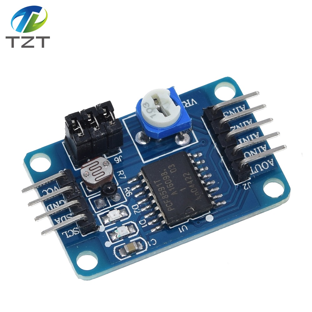
Description of two babies
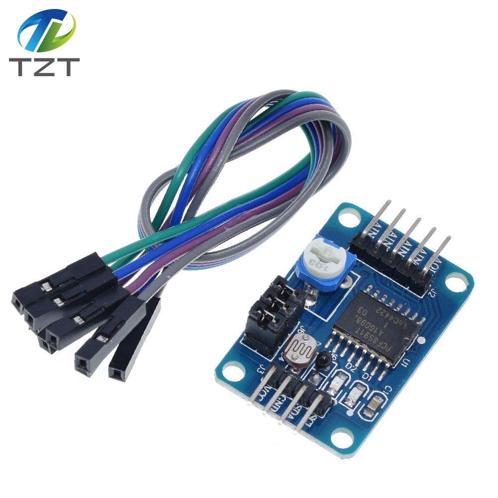
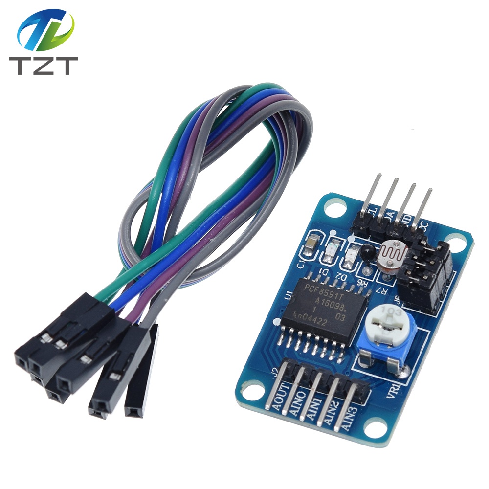
The module chip adopts PCF8951
2 module supports external 4-channel
voltage input acquisition (voltage input range 0-5v)
The 3 module integrates
photosensitive resistance, and can collect accurate value of ambient light
intensity through AD
4 module integrated thermistor, can
collect environment temperature exact value through AD
5 module integration 1 circuit 0-5v
voltage input acquisition (adjust input voltage through blue
potentiometer)
6 module with power indicator light
(after power supply to module, the indicator light will be on)
Module 7 has DA output indicator
light. When the output interface voltage of module DA reaches certain value, the
DA output indicator light on the board will be lit. The higher the voltage, the
more obvious the brightness of indicator light will be.
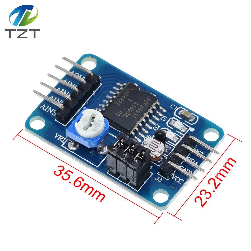
8 module PCB size: 3.6cm*2.3cm
9 standard double panel, plate
thickness 1.6mm, all around with through-hole, aperture: 3mm, easy to fix
Three module interface
description
The left and right sides of this
module are respectively expanded by 2 pin row interfaces, which are explained as
follows:
The DA output interface of the AOUT
chip on the left
AINO chip simulates input interface
0
AIN1 chip simulates input interface
1
AIN2 chip analog input interface
2
AIN3 chip analog input interface
3
On the right side, SCL IIC clock
interface is connected to MCU IO port
SDA IIC digital interface to single
chip IO port
GND module location
The VCC power interface is externally
connected to 3.3v-5v
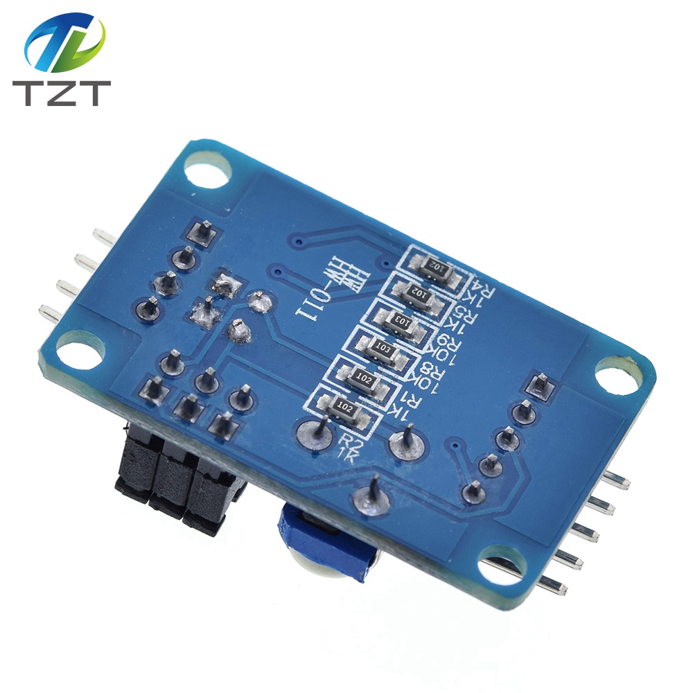
4 module red short circuit cap
instructions
The module has 3 red short circuit
caps, which are respectively used as follows:
P4 is connected with P4 short circuit
cap and thermistor is selected to access the circuit
P5 is connected with P5 short circuit
cap, and choose photosensitive resistance to access the circuit
P6 is connected with P6 short circuit
cap, and 0-5v adjustable voltage is selected to access the circuit


 TUOZHANTENG electronic components Co., LTD
 0755-82527072
 emily@tztstore.com
 3013 Hongli Road, Shanghang Building 5F/511, Huaqiangbei , Futian , Shenzhen , Guangdong , China.