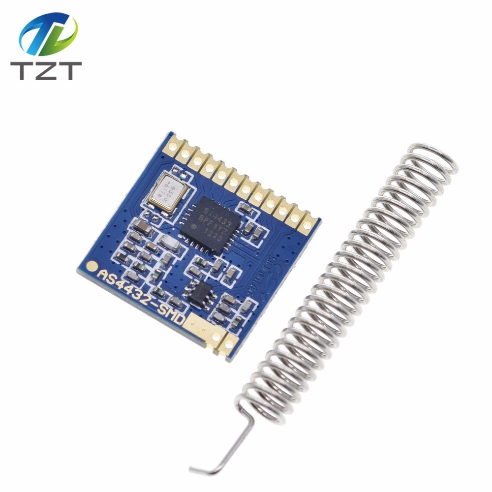
3. strong ability to penetrate 4 .ses the American SI4432 the latest version of IC, stable performance
Frequency range: 433.92M
High sensitivity up to -121dBm
Maximum output power: 20dBm
Data transfer rate: 0.123-256kbps
FSK, GFSK and OOK modulation mode
1.8-3.6 V power supply
Ultra low power off mode
The digital received signal strength indicator (RSSI)
Timing wake-up function
Automatic antenna matching and bidirectional switch control
Configurable data packet structure
Before the synchronization signal detection
64 bytes RX data register (FIFO)
Low power testing
Temperature sensing and 8 bit analog to digital converter
Operating temperature range: -20 ~ +60 C
Integrated voltage regulator
Frequency hopping
Power on reset function
Built in lens adjustment function
Pin definitions:
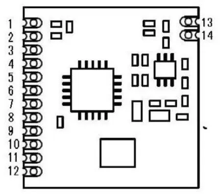
1
CND power supply
2
GPIO0 internal module, launch control foot
3
GPI01 internal access module to accept control foot
4
GPIO2 directly connected to the chip GIIO2 pin
5
VCC positive supply 3.3V
6
SDO 0-VDD V digital output provides a serial readback function of the internal
control register
7
SDI serial data input. 0-VDD V digital input, this pin for 4-wire serial data
clock function
8
SCLK serial clock input. 0-VDDV last month set of inputs. This pin provides a
4-wire serial data clock function
9
NSEL serial interface select input pin,0-VDDV digital input. This pin to 4-wire
serial data bus select / enable function, this signal is also used, said the
burst read / write mode.
10
NIRQ interrupt output pin
11
SDN Close the input pin. Input 0-VDDV digital. SDN = 0 in shutdown mode, so
mode
12
GND access power ground
13
ANT 50 ohm coaxial antenna
1.ultra-thin small 2.harmonic notes passed FCC/CE certification
3. strong ability to penetrate 4 .ses the American SI4432 the latest version of IC, stable performance
Frequency range: 433.92M
High sensitivity up to -121dBm
Maximum output power: 20dBm
Data transfer rate: 0.123-256kbps
FSK, GFSK and OOK modulation mode
1.8-3.6 V power supply
Ultra low power off mode
The digital received signal strength indicator (RSSI)
Timing wake-up function
Automatic antenna matching and bidirectional switch control
Configurable data packet structure
Before the synchronization signal detection
64 bytes RX data register (FIFO)
Low power testing
Temperature sensing and 8 bit analog to digital converter
Operating temperature range: -20 ~ +60 C
Integrated voltage regulator
Frequency hopping
Power on reset function
Built in lens adjustment function
Pin definitions:
1
CND power supply
2
GPIO0 internal module, launch control foot
3
GPI01 internal access module to accept control foot
4
GPIO2 directly connected to the chip GIIO2 pin
5
VCC positive supply 3.3V
6
SDO 0-VDD V digital output provides a serial readback function of the internal
control register
7
SDI serial data input. 0-VDD V digital input, this pin for 4-wire serial data
clock function
8
SCLK serial clock input. 0-VDDV last month set of inputs. This pin provides a
4-wire serial data clock function
9
NSEL serial interface select input pin,0-VDDV digital input. This pin to 4-wire
serial data bus select / enable function, this signal is also used, said the
burst read / write mode.
10
NIRQ interrupt output pin
11
SDN Close the input pin. Input 0-VDDV digital. SDN = 0 in shutdown mode, so
mode
12
GND access power ground
13
ANT 50 ohm coaxial antenna


China (Mainland)
 TUOZHANTENG electronic components Co., LTD
 0755-82527072
 emily@tztstore.com
 3013 Hongli Road, Shanghang Building 5F/511, Huaqiangbei , Futian , Shenzhen , Guangdong , China.
Hong Kong,China
TUOZHANTENG HK CO., LTD
1244995775@qq.com
Room 1103, Hang Seng Mongkok Building, 677 Nathan Road, Mongkok, Kowloon, Hong Kong
WhatsApp +86 15920041318
![]() WeChat +86 15920041318
WeChat +86 15920041318
Telegram/ KakaoTalk :+86 15920041318
Website customer service

Tel